NAAC-Accredited 'A++' - Grade 2(f) & 12(B) status (UGC) |ISO
9001:2015 Certified | FIST Funded (DST) SIRO(DSIR)
Electronics and Communication Engineering - Short Time Courses
Short Term Courses
A non-formal course is used to provide the knowledge plug in for the students. The additional course is conducted for the benefit of students. The courses are conducted in various domain of electronics and communication Engineering. It is a platform for the faculties to top their knowledge in latest technology.
Student should hold the core department certifications in order to get the placements in core companies. The course is useful for knowledge up gradation placements, and projects. The topics covered in the course are apart from the regular syllabus. The courses are kept on updated / newly adopted based up on recent trends. The details of currently offered course are listed.
| Duration | : | 30 Hrs | 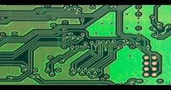 |
|---|---|---|---|
| Course Pattern | : | Evening, Weekend, Summer and Winter Holidays. | |
| Course Fee | : | Rs. 2,000/- | |
| Intake | : | 10 – 20 | |
| Eligibility | : | B. E (ECE, EEE, CSE, IT, E&I, I&C), M. E (VLSI, Communications System, Embedded System, Applied Electronics, Power Electronics, Power System,), Diploma (EEE, ECE) | |
| Prerequisite | : | Exposure on Basic Electronics. | |
| Objectives | : | Participants will be able to
|
|
| Course Content : Introduction – Component Details – Library Management – Schematic – Capture [ORCAD] – DRC and Net list creation – New part creation and loading to library – circuit simulation – basic PCB construction – linking the circuit from design – design issues – placement of components – PCB layout – manual routing – creating the new foot print – auto routing method – Fabrication method – hands on design and preparation of PCB boards. |
|||
| Course Coordinators: Mr. A. Ayubkhan. Mr. S. Sreesouthry. +91 - 427 - 4099879 | |||
| Location: Sona PCB Lab First Floor, Department of Electronics and Communication Engineering, Sona College of Technology, Salem-636005 | |||
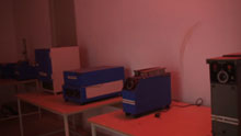
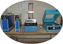
| PCB Lab facility: Printed Circuit Board laboratory focuses on training the students both in Design and Fabrication of PCB. The features and facilities available in this lab will help the students to do their projects and enhance their knowledge about the latest trends and technologies in PCBs. we are also doing fabrication of PCB based on the industry requirements. List of PCB Equipments:
|
|||
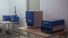
Photographs of PCB lab equipments:
| |||
| Duration | : | 30 Hrs |  |
|---|---|---|---|
| Course Pattern | : | Evening, Weekend, Summer and Winter Holidays. | |
| Course Fee | : | Rs. 1,500/- | |
| Intake | : | 10 – 20 | |
| Eligibility | : | B. E (ECE, EEE, CSE, IT, E&I, I&C), M. E (VLSI, Communications System, Embedded System, Applied Electronics) | |
| Prerequisite | : | - | |
| Objectives | : | Participants will be able to
|
|
  |
|||
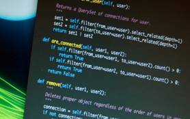
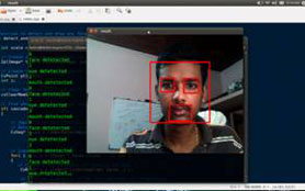
| Course Content : Introduction – open source software – Introduction on Open-CV and Python in Linux platform - basic experiments using open source – Open CV library – theory on digital image processing – hands experience on Open-CV and Python with and without library – Image classification and segmentation using Open-CV and Python. |
|||
| Course Coordinators: Mr. P. M. Dinesh. Mr. R. Anand. +91 - 427 - 4099774 |
|||
| Location: Sona DIP Lab Ground Floor, Department of Electronics and Communication Engineering, Sona College of Technology, Salem-636005 | |||
DIP Lab facility:
|
|||